|
Show content only (no menu, header)
Appendix D: Wavefront error model on optical elements
D.1 Sample PSD provided by Tinsley
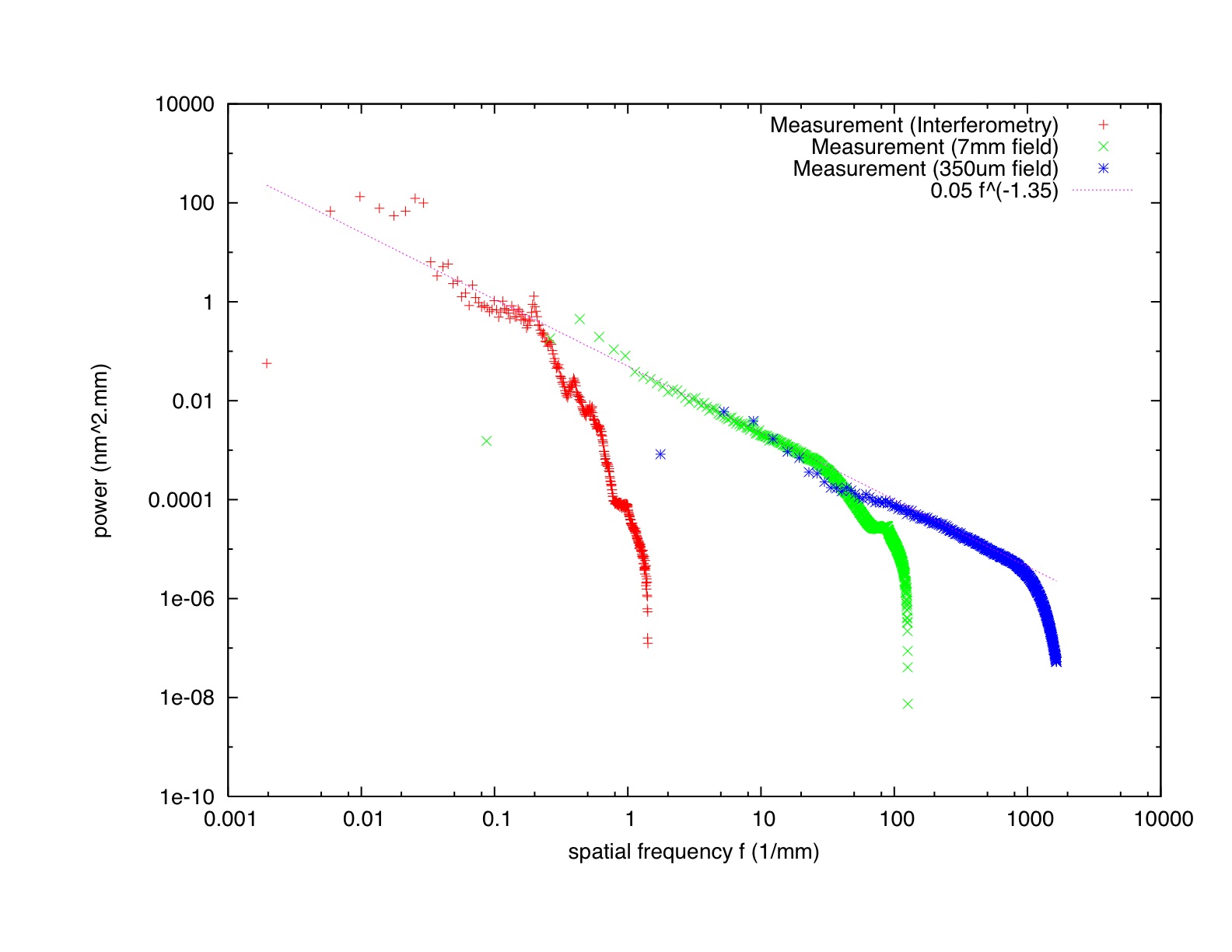 |
Figure 1: Sample PSD from a mirror similar to TMA M3 manufactured by Tinsley about 4 years ago
[jpeg]
The power law PSD (in f^-1.35) adopted for this work is the straight line in this figure.
|
The figure above shows the measured PSD of a mirror similar to TMA. The files are:
A good fit of the PSD measurement provided by Tinsley is:
|
PSD(f) = 0.05 x f-1.35
|
(equ 1)
|
|---|
Where PSD(f) is in nm2.mm, and f is in mm-1.
D.2 Surface error model adopted for M2 and M3
For both M2 and M3, the surface error is a PSD with a -1.35 power law from 10cm period to 300 μm period. The total surface error is ~ 1 nm RMS. An example surface error map generated with this model can be downloaded: aberr.fits (FITS file, 8192x8192 pix, single precision, 256 MB file size). The unit is (m) for the pixel values, and the lateral scale (x,y) is 36.6 &um;m per pixel (the full FITS file represents a 0.3m x 0.3m surface area).
Page content last updated:
27/06/2023 06:35:52 HST
html file generated 27/06/2023 06:34:40 HST
|